
Version 2 of Huawei’s "Tao Law"
Huawei's He Tingbo Releases new paper on “Tao Law”

According to the latest paper notice on ChinaXiv, the Chinese Academy of Sciences' preprint platform, Huawei semiconductor chief He Tingbo released Version 2 of Time Miniaturization Theory for Multi-Level Electronic Systems on July 3. The theory is also known in the industry as "Tao Law."
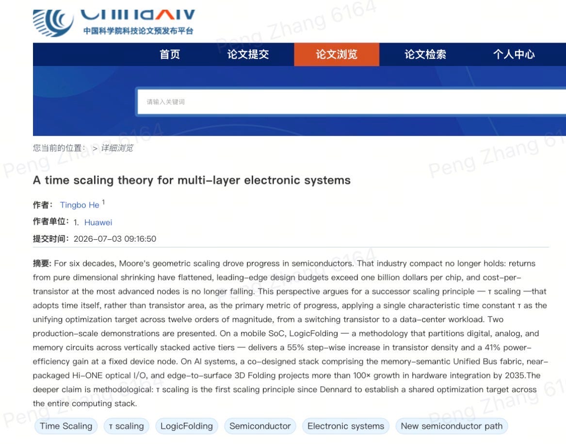
Compared with Version 1 released on May 25, the new paper adds substantial detail on engineering implementation, measured quantitative data, and product evolution roadmaps on top of the original theoretical framework. It further refines the post-Moore scaling theory system centred on the time constant τ.
On engineering implementation, Version 2 provides a more in-depth explanation of the gear ratio concept in the core technology LogicFolding. When hybrid bonding pitch approaches the size of top-level metal interconnects, the 3D design space shifts from traditional "macro-block-level discrete optimisation" to "cell-level continuous optimisation." This makes globally optimal vertical logic partitioning possible and breaks the traditional limitation of 3D stacking to functional-block-level layering only.
Version 2 also adds a new table of measured mass-production data, explicitly listing voltage, frequency, normalised power consumption, area, and power density parameters for the Kirin 2026 and the benchmark Kirin 9030 Pro.
In May this year, at the 2026 International Symposium on Circuits and Systems, He Tingbo officially introduced the "Tao (τ) Law" — the first time China had proposed an industry development guiding principle in the global semiconductor sector.
The core of the Tao Law is "time miniaturisation." Rather than simply pursuing the extreme reduction of physical dimensions, it shifts toward the systematic reduction of the time constant (τ) — compressing signal transmission delay inside chips. The framework establishes a multi-level collaborative optimisation system spanning devices, circuits, chips, and systems. By 2031, high-end chips based on this law are projected to reach transistor density equivalent to the 1.4 nm process node.